
-
Highlight
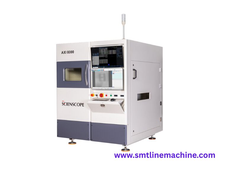
Scienscope X-RAY 3D AXI 8000 machine
,fully automatic SMT line machine
,3D AXI X-RAY inspection system
-
Place of OriginCHINA
-
Brand NameScienscope
-
CertificationCE
-
Model NumberX-RAY 3D AXI 8000 Fully Automatic
-
Minimum Order Quantity1 set of machine or mixed order is also acceptable
-
PriceNegotiable
-
Packaging DetailsStandard export boxes and sturdy hardwood packages are both options
-
Delivery Time5-8 Working days
-
Payment TermsL/C, D/A, D/P, T/T, Western Union,MoneyGram
Scienscope X-RAY 3D AXI 8000 Fully Automatic HIGH END
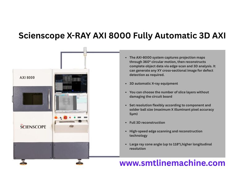
The Scienscope X-RAY 3D AXI 8000 Fully Automatic is an entirely automated 3D X-ray inspection system that utilizes sophisticated CT (Computed Tomography) technology. This advanced scanner provides a complete 360-degree view within your electronic components without requiring disassembly.
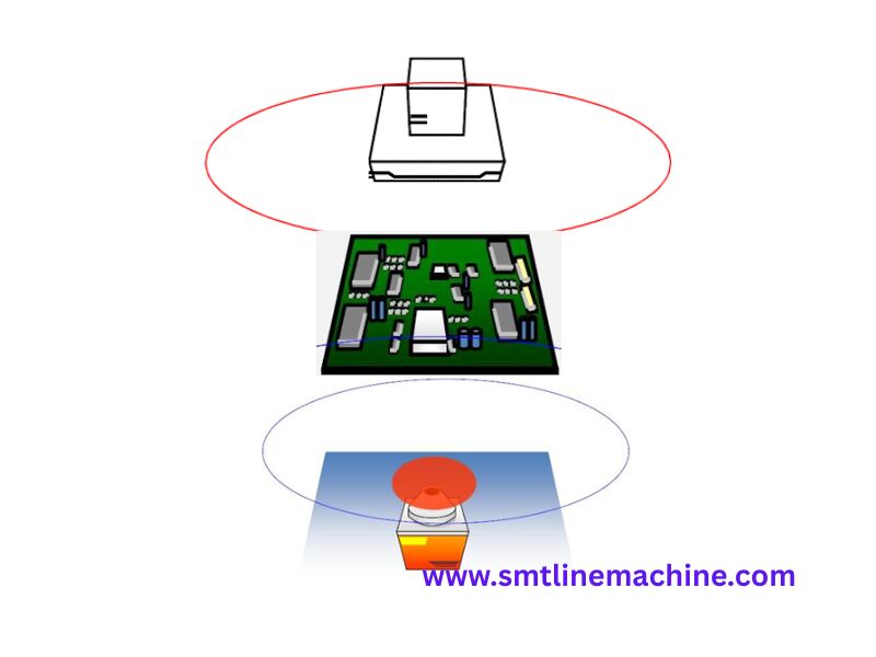
The system captures projection mappings by rotating around the object in a full circle, then employs edge-scan and 3D analysis techniques to reconstruct all collected data. This creates a digital 3D replica that allows examination of internal structures from any perspective to identify even the tiniest defects.
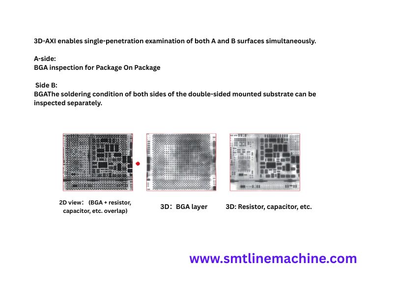
3D Automated X-ray Inspection (AXI) represents a cutting-edge approach in electronics manufacturing, designed to deliver comprehensive evaluations of Printed Circuit Boards (PCBs). Unlike conventional 2D X-ray methods, 3D AXI leverages computed tomography (CT) to produce detailed, three-dimensional visualizations of the internal composition of electronic components and solder connections. This sophisticated technique identifies defects undetectable via 2D X-ray, including voids, misalignments, and inadequate solder application.
| Parameter Category | Specification | Details |
|---|---|---|
| X Illuminant | Light tube voltage, current | 130KV 300uA |
| Maximum Output | 39W | |
| FPD | Resolution ratio | 50um |
| Frame Rate | 1x1 9fps, 2x2 18fps | |
| Pixel Size | 2340x2882 | |
| CCD Camera | Pixel | 2.3 megapixel |
| Function | Scan the barcode | |
| CT Parameters | Resolution ratio | 5um |
| Number of Projections | 32,64,120 | |
| Shooting Angle | 60°, 90° | |
| Maximum Number of Layers | Unlimited (recommended <300) | |
| Test Parameters | Feed height | 85mm on top, 20mm on bottom |
| Delivery Direction | Left in, right out | |
| PCB Size | 100x50-400x400 | |
| Circuit Board Thickness | ≥0.5mm | |
| Height of Test Object Components | 85mm on top, 20mm on bottom | |
| Object Weight | ≤5KG | |
| FOV Size | 58x70mm (25μm precision), 11x14mm (5μm precision) | |
| Plate Bending Correction | Hardware correction | |
| Safety | Radiation | 1μSv/H |
| Safety Interlocking | Available | |
| Environmental Requirements | Working Temperature | 0-40℃ |
| Working Humidity | 40%-60% | |
| Working Power Supply | 220V | |
| Aggregate Capacity | 2KW | |
| Pressure Requirements | 0.4-0.6 MPa | |
| Load Capacity Requirements | 1.5T/㎡ | |
| Device Appearance | Size | 1625mm*1465mm*1905mm |
| Weight | 2.5T |
- Extensive Flaw Detection: Identifies a broad spectrum of defects including solder joint integrity issues, component displacement, air pockets, and concealed electrical short circuits.
- High-Resolution Imaging: Employs advanced X-ray cameras and sophisticated algorithms to secure detailed imagery for critical insights into PCB internal architecture and robustness.
- Streamlined Efficiency and Usability: Equipped with intuitive interfaces and user-friendly software for straightforward operation and rapid inspection cycles to boost production throughput.
- Automated Calibration: Features automatic adjustment of inspection parameters to accommodate production changes, minimizing setup losses and manual recalibrations.
- Complete 3D X-Ray Analysis: Offers full 3D reconstruction for thorough assessment.
- Non-Invasive Assessment: Allows inspection of circuit boards without inducing damage.
- Adaptable Layer Selection: Permits selection of necessary layers for examination.
- Customizable Resolution: Enables adjustment of resolution based on component dimensions and solder balls, ensuring precision.
- Accelerated Edge Scanning: Incorporates rapid scanning and reconstruction technologies.
- Broad Ray Cone Angle: Delivers superior longitudinal resolution for enhanced inspection.
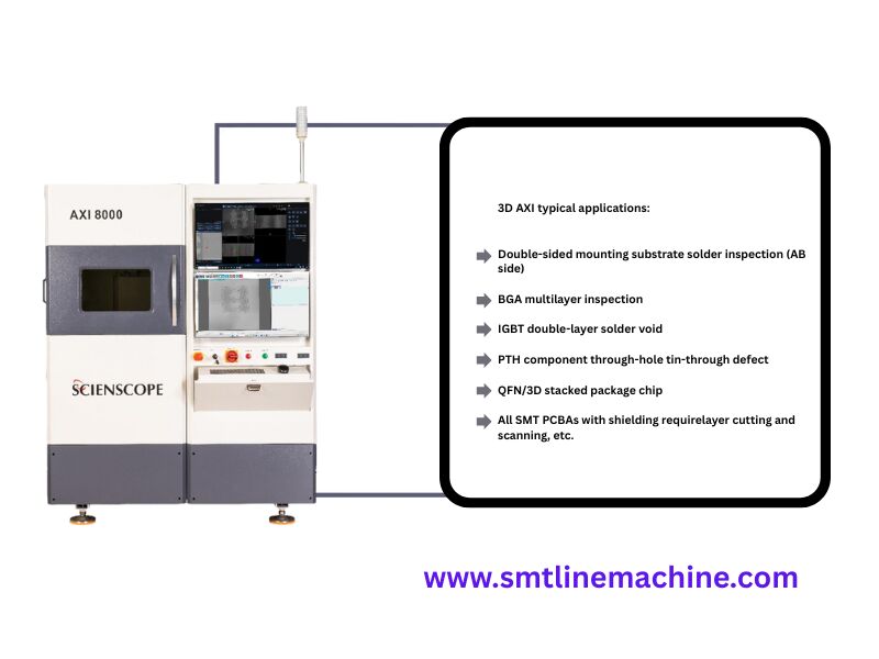
- Inspection of Surface Mount Technology (SMT) and Through-Hole Components: Guarantees quality of solder joints and precision of component placement in both SMT and through-hole assemblies.
- Examination of Ball Grid Arrays (BGAs) and Press-Fit Connectors: Detects faults in BGA solder joints and verifies integrity of press-fit connections.
- Dual-Sided PCB Analysis: Evaluates both faces of double-sided PCBs to ensure uniform quality standards.
- Computed Tomography (CT): Utilizes X-rays to create sectional images compiled into 3D representations.
- High-Definition X-Ray Cameras: Capture intricate images of internal structures of electronic parts.
- Automated Anomaly Recognition (AAR): Employs software algorithms to automatically identify defects through image analysis.
- Real-Time Oversight and Management: Empowers operators to supervise inspection processes and implement adjustments as required.
- Enhanced Quality Assurance: Identifies defects early in production, preventing circulation of defective products.
- Amplified Productivity: Automates inspection workflow, reducing manual labor and accelerating production speeds.
- Economical Benefits: Lowers waste and rework needs by spotting defects before they escalate.
- Heightened Dependability: Confirms electronic goods adhere to highest quality and reliability benchmarks.
Scienscope X-RAY AXI 8000 3D AXI systems are indispensable for upholding the quality and dependability of electronic products. By supplying comprehensive three-dimensional imagery of internal structures, these systems enable manufacturers to uncover defects that might otherwise go unnoticed.
For inquiries, please contact us at:
Phone: +8613537875415
Email: Lizzy@smtlinemachine.com
Address: Xintian Industrial Area, Baoan, Shenzhen City, China
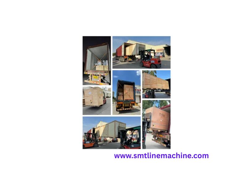
- Delivery: 5-8 business days (varies based on order quantity)
- Minimum Order: Single machine or mixed orders accepted
- Transportation: Bulk shipping or container shipment based on order size
- Payment Terms: L/C, D/A, D/P, T/T, Western Union, MoneyGram
- Price: Negotiable for best value
- Packaging: Standard export boxes or robust hardwood packages for safe delivery
Our products are sold all over the world, you can rest assured.