
-
Highlight
heller reflow oven
,lead free reflow ove
-
BrandCNSMT
-
MODELCN-B8810-LF
-
Weight800KG
-
Lead TimeIN Stork
-
PackingWOODENBOX
-
POWER3-phase 5-wire 380V
-
PCB WIDTH50-350MM
-
PAYMENT TERMT/T, Paypal, Westernunion Are All Allowed
-
Place of Originchina
-
Brand NameCNSMT
-
CertificationCE
-
Model NumberCN-B8810-LF
-
Minimum Order Quantity1
-
Pricenegotiation
-
Packaging Detailswoodenbox
-
Delivery Time5-7 work days
-
Payment TermsT/T, Western Union
-
Supply Ability10pcs/day
8 Heating Zones SMT Reflow Oven Soldering 380V For Led PCB Board
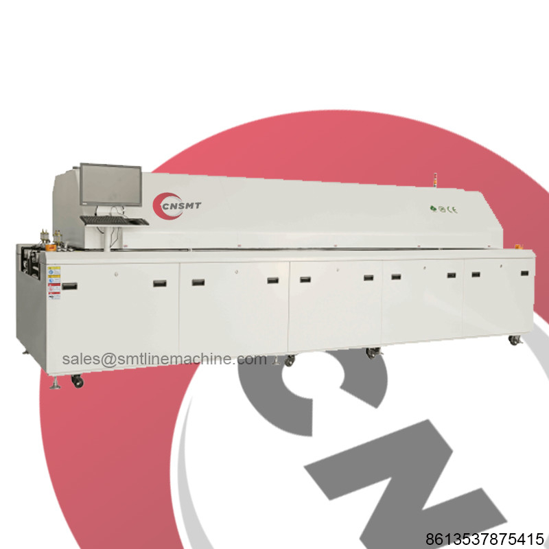
8 heating zones smt reflow oven led PCB board reflow soldering machine 1year warranty
Specification:
| Main control module | PLC and temperature control module |
| Computer control host, monitor | Lenovo |
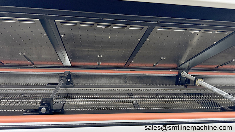
| Number of heating zones | There are 8 small circulation heating areas on the top and 8 small circulation heating areas on the bottom. |
| Heating zone length | 3140MM |
| Number of cooling zones | 2 independent cooling zones + 1 external air cooling system |
| Cooling zone length | (350*2)+600 mm |
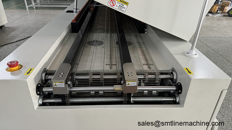
| Conveyor belt width | 450 mm |
| Guide rail width adjustment range | 50~320mm |
| PCB size | 50-320mm |
| PCB height limit | 25mm |
| Transmission direction | L-R (R—L) direction can be selected before manufacturing |
| Transmission method | Mesh belt + guide rail |
| Conveyor belt height | 900±20mm |
| PCB transportation speed | 0~1.8m/min |
| Temperature control accuracy | ±1-2℃(static) |
| temperature control range | Room temperature ~ 300℃ can be set |
| Applicable solder type | Lead-free solder/lead solder |
| Temperature control method | PID+SSR |
| Type of components used | CSP, BGA, μBGA, 0201chip and other single/double panels |
| Abnormal alarm | Abnormal temperature (over-temperature alarm after constant temperature) |
| Power outage protection | UPS effectively prevents PCB boards from being burned out during sudden power outages. |
| power supply | 3Φ, 380V, 50HZ |
| Starting power | 38KW |
| Working power | 8KW |
| Heating time | Approx.20min |
| Dimensions | L4800*950*1450 mm |
| net weight | 1200kg |
![]()
Technical Features of the Machine:
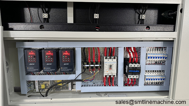
1. **Intelligent Control System**:
- Utilizes Lenovo computer and PLC intelligent control system with a temperature control accuracy of up to ±1-2℃.
- Even in the event of computer failure, offline operation can be achieved without affecting production, ensuring stable and reliable control system operation.
2. **Operating Interface**:
- Windows 7 operating system with powerful functionality and user-friendly interface for enhanced operational efficiency.
3. **Safety Design**:
- The lifting mechanism of the upper furnace body employs automatic cylinder lifting and is equipped with safety support rods to ensure safe and reliable operation.
- Features fault alarm functions and leakage protection devices to ensure the safety of operators and the control system.
4. **Stable Transport System**:
- Equipped with a mesh belt tensioning device to ensure smooth, vibration-free, and deformation-free transportation of PCBs.
- Utilizes synchronous rail transport mechanism, allowing precise adjustment of the rail width and ensuring high longevity, with the capability to interface with fully automatic chip mounters.
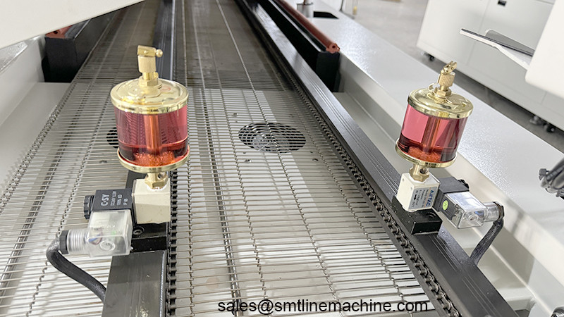
5. **Lubrication System**:
- Incorporates an automatic lubrication system that enables automatic lubrication of transmission chains by setting lubrication time and volume.
6. **Temperature Control**:
- All heating zones are PID-controlled by the computer, with independent temperature control for the upper and lower zones to achieve high-precision temperature control.
- Each temperature zone is equipped with independent temperature sensing sensors for real-time monitoring and compensation of temperature imbalances.
7. **Emergency Shutdown Protection**:
- Built-in UPS automatic delay shutdown system to ensure equipment integrity in the event of power failure or overheating.
8. **Efficient Heating System**:
- Adopts the world's leading small cycle heating method, with independent upper and lower hot air small cycle systems for uniform temperature distribution and high thermal compensation efficiency.
- Equipped with a high-efficiency pressurized air duct to significantly increase the circulation of hot air and achieve rapid temperature rise.
9. **Process Parameter Management**:
- Features a password-protected operating system to prevent unauthorized personnel from modifying process parameters.
- Operation record management allows for the tracing of process parameter changes, facilitating process improvement.
10. **Rapid Cooling System**:
- Incorporates an emergency cooling system based on international advanced technology, achieving cooling rates of up to 3.5~6℃/sec.
- Optional external forced cooling devices are available to ensure optimal solder crystallization effects.
11. **Rosin Recovery System**:
- Rosin flows directionally for easy replacement and cleaning, with dedicated pipelines for exhaust gas transmission, requiring no maintenance throughout its lifetime.
12. **Quiet Design**:
- Special pressurized air delivery structure and unique heating wire design ensure noise-free and vibration-free operation, providing a quiet working environment.
The comprehensive application of these technical features results in outstanding performance and stable operational efficiency of our product, meeting various production requirements and delivering higher production value to our customers.
![]()
![]()
Company Information
CNSMT is the leading manufacturer and supplieir for SMT machines and Solution with over 10 years' experience in China. And we can also do OEM&ODM for SMT traders, we have vast of sources in SMT field,even you need used or new SMT equipments or other parts, we can help you get the best quality and competitive cost machines.
What we can do for you:
※ We have our own factory make SMT equipments and devices
※ We have a professional technich engineer team for produce machines
※ We can customize variety of SMT machines for you according your requirements
※ We buy and sell used and new SMT equipments all over the world
※ We provide you SMT full line machines and export to worldwide
※ Becoming the most reliable Chinese partner for you.
![]()
Our products are sold all over the world, you can rest assured.