OEM ODM android development PCB board Multilayer PCB Board manufacturer
Quick Detail
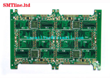
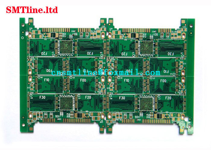
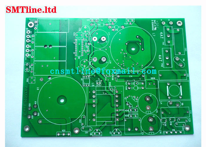
| Product Name: | SMD LED PCB Board |
| Used for: | SMT FACTORY Electronic Circuit Board |
| Warranty: | 1 Year |
| Shipment | by air |
| Delivery Time: | 1-2Days |
| Our Main Market | Whole of the world |
Less vias
Once the via is selected, the clearance between it and the surrounding entities must be properly handled, especially the gaps between the lines and vias that are easily disconnected and the vias are not connected to the vias. If the wiring is automatic, the number of vias can be The "On Minimiz8tion" sub-menu selects the "on" item to automatically resolve. (2) The larger the required ampacity, the greater the size of the required vias, and the larger vias used for the connection of the power plane and the formation to other layers.
Silk screen
Overlay
In order to facilitate the installation and maintenance of the circuit, the required logo patterns and character codes and the like are printed on the upper and lower surfaces of the printed board, such as component labels and nominal values, component outline shapes, and manufacturer's marks, production dates, and the like. When many beginners design the silkscreen layer, they only pay attention to the neat appearance of the text symbols, and ignore the actual PCB effects. On the printed boards they designed, the characters were not blocked by the components or they were invaded by the soldering area, and the components were indexed on the adjacent components. All of these designs would bring about great assembly and maintenance. inconvenient. The correct layout principle of the silk screen layer is: "No ambiguity, no seams, beautiful appearance."
SMD package
Speciality
Protel package library has a large number of SMD packages, surface mount devices. The biggest feature of this type of device is that it is a single-sided distributed elemental pinhole. Therefore, the surface of the device should be defined so as to avoid "missing pins". In addition, the relevant text labels of such components can only be placed along the surface of the component.
Fill area
External Plane and Fill
As the name of both, the network-like filling area is to treat a large area of copper foil as a mesh, and the filling area is only a complete reserved copper foil. In the process of designing beginners, you often cannot see the difference between the two in the computer. In essence, as long as you enlarge the drawing, you can see it at a glance. It is because it is not easy to see the difference between the two, so the use of time does not pay much attention to the distinction between the two, to emphasize that the former has a strong role in inhibiting high-frequency interference in the circuit characteristics, apply to need to do Areas where large areas are filled are particularly appropriate when certain areas are used as shielding, partitions, or high-current power lines. The latter is often used in places where small filling is required, such as a general line end or a transition area.
Pad
Pad
Pads are the most common and most important concept in PCB design, but beginners tend to overlook their choices and fixes, and use circular pads in the design. The pad type of the selected component must consider the shape, size, layout, vibration and heat conditions, and force direction of the component. Protel gives a series of pads of different sizes and shapes in the package library, such as circles, squares, octagons, circles, and positioning pads, but sometimes this is not enough and you need to edit it yourself. For example, for a pad that generates heat and is subject to greater force and current, it can be designed as a “teardrop”. In the familiar color TV PCB output transformer pin pad design, many manufacturers are Adopt this form. In general, besides the above, the following principles should be considered when editing the pad by yourself:
(1) When the length of the shape is inconsistent, consider that the difference between the width of the connecting line and the length of the specific side of the pad should not be too large;
(2) The need to use asymmetrical pads of long and short lengths when routing between component lead angles is often more effective;
(3) The size of each component pad hole should be edited and determined according to the component pin thickness. The principle is that the hole size is 0.2-0.4 mm larger than the pin diameter.
Our products are sold all over the world, you can rest assured.