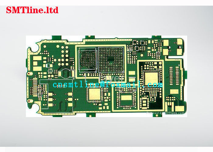

CNSMT Custom Wifi Router SMD LED PCB Board Electronic Circuit Board Factory price
Quick Detail
Feature
| Product Name: | SMD LED PCB Board |
| Used for: | SMT FACTORY Electronic Circuit Board |
| Warranty: | 1 Year |
| Shipment | by air |
| Delivery Time: | 1-2Days |
| Our Main Market | Whole of the world |
Application
The design of the printed circuit board is based on the circuit schematic and implements the functions required by the circuit designer. The design of the printed circuit board mainly refers to the layout design, and the layout of the external connection needs to be considered. The optimal layout of internal electronic components. Metal wiring and through hole optimization layout. Electromagnetic protection. Heat dissipation and other factors. Excellent layout design can save production costs and achieve good circuit performance and thermal performance. Simple layout designs can be implemented manually, and complex layout designs require computer-aided design (CAD).
In high-speed designs, the characteristic impedance of controlled impedance boards and lines is one of the most important and common problems. First understand the definition of the transmission line: The transmission line consists of two conductors of a certain length, one conductor is used to send signals, and the other is used to receive signals (remember the notion of "circuit" instead of "ground"). In a multilayer board, each line is part of a transmission line, and the adjacent reference plane can be used as a second line or loop. A line a "good performance" it is critical transmission line characteristic impedance of the entire circuit remains constant. [1]
The key to the circuit board being a "controlled impedance board" is to make the characteristic impedance of all lines meet a specified value, usually between 25 ohms and 70 ohms. In a multilayer circuit board, the key to good performance of the transmission line is to keep its characteristic impedance constant throughout the entire line.
But what exactly is characteristic impedance? The easiest way to understand the characteristic impedance is to see what the signal encounters during transmission. When moving along a transmission line with the same cross-section, this is similar to the microwave transmission shown in FIG. Assume that a step voltage of 1 volt is applied to this transmission line, such as a 1 volt battery connected to the front end of the transmission line (it is located between the transmission line and the return line). Once connected, this voltage wave signal follows the line at the speed of light. Spread, its speed is usually about 6 inches/nanoseconds. Of course, this signal is indeed the voltage difference between the transmission line and the loop, which can be measured from any point on the transmission line and the point of the loop. FIG. 2 is a schematic diagram of the transmission of the voltage signal.
Zen's method is to "generate a signal" first, and then spread along this line at a speed of 6 inches/nanoseconds. The first 0.01 ns advances by 0.06 inches. At this time, the sending line has an extra positive charge, and the circuit has an extra negative charge. It is these two kinds of charge differences that maintain a voltage difference of 1 volt between the two conductors. The two conductors form a capacitor.
In the next 0.01 nanosecond, the voltage of a 0.06 inch transmission line is also adjusted from 0 to 1 volt, which must add some positive charge to the transmission line and add some negative charge to the receiving line. For every 0.06 inches of movement, more positive charge must be added to the transmission line, and more negative charge must be added to the circuit. Every 0.01 nanosecond, another section of the transmission line must be charged and then the signal begins to propagate along this section. The charge comes from the battery at the front end of the transmission line. When moving along this line, it charges a continuous portion of the transmission line, thus creating a voltage difference of 1 volt between the transmission line and the loop. Every 0.01 nanosecond advances, some charge (±Q) is obtained from the battery, and the constant charge (±Q) flowing out of the cell over a constant time interval (±t) is a constant current. The negative current flowing into the loop is actually equal to the positive current flowing out, and just in front of the signal wave, the alternating current passes through the capacitance formed by the upper and lower lines, ending the entire cycle.
Our products are sold all over the world, you can rest assured.